Semiconductor Services

Equipment control design, development, and testing

Equipment control design, development, and testing

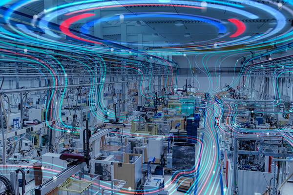
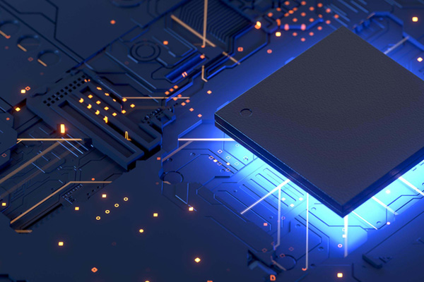
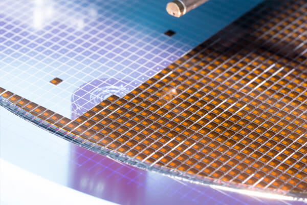
Semiconductor development and design involves a lot of elements, the design and development process will be carried out in a controlled manner. RTL design and Physical design will be carried out in the development stage. The development and design stages will be monitored by the operator. The digital section of the design can be defined by RTL programming. IoT is used to implement the data transfer and thereby we can easily determine any faults. We use Automated test equipment to check the semiconductor.

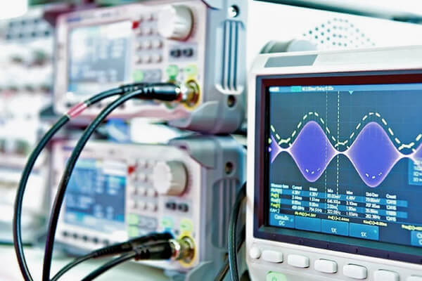
Electronic design automation is utilised to do the designing and simulation. We will be able to check several data while using the EDA. Electronic software design tools such as Proteus and Eagle will help us to execute the designing process efficiently.

Industry-leading Framework integration (Cimmetrix, Peer Tool Orchestrator, etc)

We are using the Cimmetrix and Peer Tool orchestrator and these are equipment control software frameworks. Supervisory control can be achieved with the help of these frameworks. So equipment automation can be done by using these frameworks.

Semiconductor testing is carried out by using Automation test equipment. We can test several electronic devices by using this machinery and thereby determine the quality of the product.
Firmware is the software that is used with the test equipment and other devices in the manufacturing plant. The firmware will provide several instructions to the devices and based on that the operations will be carried out.

Factory automation will reduce human intervention in the manufacturing process. Artificial intelligence, IIoT, and firmware software are used in this process. Due to this a lot of manufacturing processes can be carried out effectively.

In semiconductors, manufacturing automation plays a great role from design to development. There are several steps in the semiconductor manufacturing process such as deposition, ionisation, etc, and all of these can be easily carried out with factory automation.

Semiconductor development involves a lot of hardware and all these devices can be integrated together to achieve good control in the semiconductor development stage. Firmware is used to do the hardware integration; a lot of devices can be controlled by using firmware. We can add the firmware software to the hardware without making any physical changes to the hardware. We are capable of embedding the firmware into the required hardware. Mostly we use python and Embedded C to program the firmware.

During the semiconductor manufacturing process, quality is an important factor. The manufactured semiconductor will be mostly for integrated circuits and then it will be utilised in PCB. So different types of cameras are used to determine the quality of the semiconductor. Semiconductor manufacturing is a complex process and because of this, EDA is used in most of the design and manufacturing sectors. Electronic Design Automation(EDA) plays a great role in semiconductor manufacturing. We are implementing this to achieve proper quality during the development stage of the semiconductor.

Artificial intelligence makes the semiconductor manufacturing process simple and will be useful to determine the defective raw material. The manufacturing process can be digitised by using AI. Mostly the designing part is carried out by utilising AI and ECAD. ECAD and AI are useful for 3D designing and this will provide us with a clear-cut image of how the end product will turn out.

SCADA is utilised to achieve supervisory control in the manufacturing industry. We also use IPC which are industrial computers that are used to control several types of machinery. Open Platform Communication is used to carry out industrial communication.

EDA will improve the communication between the factory equipment and software applications in a factory. Data transfer will be easily carried out due to the EDA interface. The designing process utilises several software. The communication between the machinery and the monitoring system can be easily achieved by the EDA interface.

Several pieces of equipment will be used during the manufacturing of the semiconductor. We do integrate all this equipment to operate together with the help of automation.

We are using AI in our industrial process and this will be useful for analysing the data based on the factory operations. Several faults can be prevented before they can even arise. EDA interface and IIOT will be useful to transfer the data really quickly and this will be really useful to analyse the data regarding the designing and manufacturing of the semiconductor. There are several EDA software tools utilised to determine the performance and quality of the design and product. All these will be useful to prevent several faults.

A semiconductor is an integral part of an IC. Integrated circuits are the major component in an electronic device, wafer recovery plays an important role in IC fabrication. We also do wafer recovery.

See who’s changed their own future
We’ve got decades-long relationships with the biggest brands in the world.